- 您现在的位置:买卖IC网 > Sheet目录316 > BR34L02FV-WE2 (Rohm Semiconductor)IC EEPROM 2KBIT 400KHZ 8SSOP
BR34L02FV-W
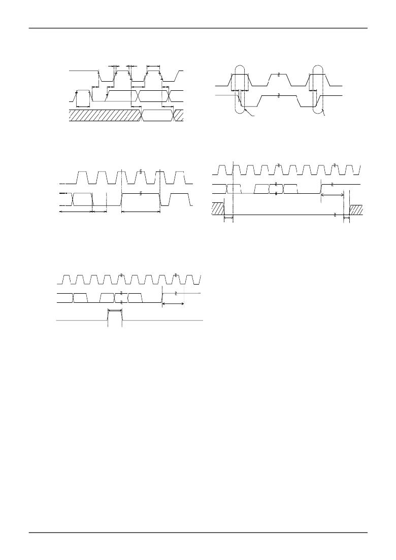
● Synchronous Data Timing
Technical Note
tR
tF
tHIGH
SCL
SCL
tHD:STA
tSU:DAT tLOW
tHD:DAT
SDA
tSU:STA
tHD:STA
tSU:STO
(IN)
SDA
(OUT)
tBUF
tPD
tDH
SDA
START BIT
STOP BIT
Fig.1-(a) Synchronous Data Timing
○ SDA data is latched into the chip at the rising edge ○
of SCL clock.
○ Output data toggles at the falling edge of SCL clock.
SCL
Fig.1-(b) Start/Stop Bit Timing
SCL
DATA(1)
DATA(n)
SDA
D0
ACK
SDA
D1
D0
ACK
ACK
t WR
WRITE DATA(n)
STOP CONDITION
t WR
START CONDITION
WP
tSU : WP
Stop Condition
t HD : WP
SCL
Fig.1-(c) Write Cycle Timing
Fig.1-(d) WP Timing Of The Write Operation
DATA(1)
DATA(n)
SDA
D1
D0
ACK
ACK
tHIGH:WP
tWR
WP
Fig.1-(e) WP Timing Of The Write Cancel Operation
○ For WRITE operation, WP must be "Low" from the rising edge of the
clock (which takes in D0 of first byte) until the end of tWR. (See
Fig.1-(d) ) During this period, WRITE operation can be canceled by
setting WP "High". ( See Fig.1-(e) )
○ When WP is set to "High" during tWR, WRITE operation is
immediately ceased, making the data unreliable. It must then be
re-written.
www.rohm.com
? 2009 ROHM Co., Ltd. All rights reserved.
3/17
2009.04 - Rev.A
发布紧急采购,3分钟左右您将得到回复。
相关PDF资料
BR93L76RFVJ-WE2
IC EEPROM 8KBIT 2MHZ 8TSSOP
BS08D-112
TRIGGER BILTRL SW 175MA TO-92
BU04P-TZ-S
TZ CONN 4 POS SINGLE ROW
BU9829GUL-WE2
IC EEPROM 16KBIT SPI 9VCSP
BU9832GUL-WE2
IC EEPROM 8KBIT SPI VCSP50L2 TR
BU9833GUL-WE2
IC EEPROM 2KBIT 100KHZ VCSP50L1
BU9844GUL-WE2
IC EEPROM 16KBIT 2WIRE VCSP50L1
BU9847GUL-WE2
IC EEPROM 4KBIT 2WIRE VCSP50L1
相关代理商/技术参数
BR34L02-W
制造商:ROHM 制造商全称:Rohm 功能描述:2Kbit Serial I2C BUS EEPROM For SPD DRAM Memory Module
BR34-UPC
制造商:Thomas & Betts 功能描述:GROUND ROD CLAMP 3/4 BRONZE
BR35
制造商:PANJIT 制造商全称:Pan Jit International Inc. 功能描述:MINI SURFACE MOUNT SCHOTTKY BARRIER RECTIFIER
BR-35
制造商:LUGUANG 制造商全称:Shenzhen Luguang Electronic Technology Co., Ltd 功能描述:Single-phase Silicon Bridge Rectifier
BR350
制造商:Eaton Corporation 功能描述:Type BR Breaker 50A/3 Pole 240V 10K
BR3500
制造商:EIC 制造商全称:EIC discrete Semiconductors 功能描述:SILICON BRIDGE RECTIFIERS
BR3500_05
制造商:EIC 制造商全称:EIC discrete Semiconductors 功能描述:SILICON BRIDGE RECTIFIERS
BR35005
制造商:BILIN 制造商全称:Galaxy Semi-Conductor Holdings Limited 功能描述:SILICON BRIDGE RECTIFIERS
